(China (Mainland))

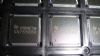
Product Summary
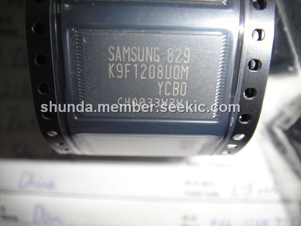
The K9F1208U0M-YCB0 is a 64M(67,108,864)x8bit NAND Flash Memory with a spare 2,048K(2,097,152)x8bit. Its NAND cell provides the most cost-effective solution for the solid state mass storage market. Even the write-intensive systems can take advantage of the K9F1208U0M-YCB0’s extended reliability of 100K program/erase cycles by providing ECC(Error Correcting Code) with real time mapping-out algorithm. The K9F1208U0M-YCB0 is an optimum solution for large nonvolatile storage applications such as solid state file storage and other portable applications requiring non-volatility.
Parametrics
K9F1208U0M-YCB0 absolute maximum ratings: (1)Voltage on any pin relative to VSS:-0.6V to + 4.6V; (2)Temperature Under Bias:-10℃ to +125℃; (3)Storage Temperature:-65℃ to +150℃.
Features
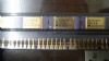
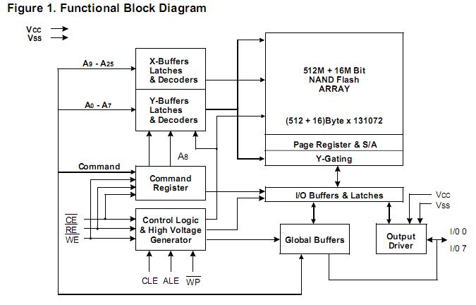
K9F1208U0M-YCB0 features: (1)Voltage Supply: 2.7V to 3.6V; (2)Organization: Memory Cell Array : (64M + 2,048K)bit x 8bit, Data Register : (512 + 16)bit x8bit multipled by four planes; (3)Automatic Program and Erase: Page Program : (512 + 16)Byte, Block Erase : (16K + 512)Byte; (4)528-Byte Page Read Operation: Random Access : 12ms(Max.), Serial Page Access : 50ns(Min.); (5)Fast Write Cycle Time: Program time : 200ms(Typ.), Block Erase Time : 2ms(Typ.); (6)Command/Address/Data Multiplexed I/O Port; (7)Hardware Data Protection:Program/Erase Lockout During Power Transitions; (8)Reliable CMOS Floating-Gate Technology: Endurance : 100K Program/Erase Cycles, Data Retention : 10 Years; (9)Command Register Operation; (10)Intelligent Copy-Back Operation; (11)Package : 48-Pin TSOP I (12 x 20 / 0.5 mm pitch); (12)Simultaneous Four Page/Block Program/Erase.
Diagrams
 |
 K9F1208D0A |
Other |
|
Data Sheet |
Negotiable |
|
||||
|
K9F1208Q0A-XXB0 |
Other |
|
Data Sheet |
Negotiable |
|
||||
|
K9F1208Q0B |
Other |
|
Data Sheet |
Negotiable |
|
||||
|
K9F1208R0B |
Other |
|
Data Sheet |
Negotiable |
|
||||
|
K9F1208U0A |
Other |
|
Data Sheet |
Negotiable |
|
||||
|
K9F1208U0A-VCB0 |
Other |
|
Data Sheet |
Negotiable |
|
||||